永大環保
廢樹酯.離子交換樹脂.壓克力樹脂.廢油泥.廢油墨.廢溶劑.廢酸液.廢鹼液.廢膠.廢汙泥.廢水.廢木材.玻璃纖維.廢塑膠.廢藥渣.廠房拆除.生活垃圾等各種工業廢棄物處裡(申報代碼C-D類)~回收電子零件.電線.五金.貴金屬.含金物.庫存品.設備機台.電腦週邊商品.工廠下腳料.光電相關原件等資源回收物品.歡迎公司行號.機關團體來電洽詢指教 謝謝
曾先生:0931079790
電 話:03-4985998
傳 真:03-4986558
公司網址: http://www.yung-da.tw
廢樹酯.離子交換樹脂.壓克力樹脂.廢油泥.廢油墨.廢溶劑.廢酸液.廢鹼液.廢膠.廢汙泥.廢水.廢木材.玻璃纖維.廢塑膠.廢藥渣.廠房拆除.生活垃圾等各種工業廢棄物處裡(申報代碼C-D類)~回收電子零件.電線.五金.貴金屬.含金物.庫存品.設備機台.電腦週邊商品.工廠下腳料.光電相關原件等資源回收物品.歡迎公司行號.機關團體來電洽詢指教 謝謝
曾先生:0931079790
電 話:03-4985998
傳 真:03-4986558
公司網址: http://www.yung-da.tw
上一頁下一頁
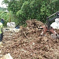
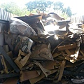
廢樹枝清除

工廠下腳料回收買賣

矽廢料處理清除
離子交換樹酯處理清除
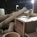
FRP風管處理(玻璃纖維)

FRP風管

pc版回收

PC版回收
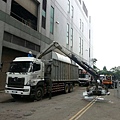
夾子車外叫服務

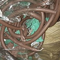
電線回收買賣

電線回收買賣

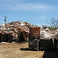
廠房拆除

夾子車外叫服務

廠房拆除

廠房拆除
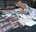
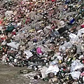
廢紙回收買賣

廢塑膠處理

廢樹脂處理

廠房拆除
廢樹脂處理

廢甲苯事業廢水

廠房拆除
廠房拆除

氯苯蒸餾殘渣處理

廢膠處理
廢硝酸處理

電線回收買賣

廢玻璃處理
廢電池回收買賣

廢電池回收買賣

廢鐵回收買賣

電線皮處理
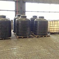
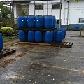
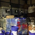
一頓桶回收買賣

機械設備回收買賣

塑膠回收買賣

過期商品銷毀

玻璃纖維處理

混和五金回收買賣

機械設備回收買賣

廢鐵回收買賣

混合五金回收買賣
0013廢橡膠處理

治具回收買賣

混合五金回收買賣

靜電袋處理

混合五金回收買賣

電子庫存回收買賣
面板玻璃處理

廢溶劑處裡

油性丙烯處理

混合五金回收買賣
偏光片處理

PC版回收買賣

電腦周邊回收買賣

廢塑膠處理

顯示卡回收買賣

玻璃纖維處裡

顯示卡回收買賣

玻璃纖維絲處理

機械設備回收買賣

玻璃纖維處理

機械設備回收買賣

0023玻璃纖維
破碎機回收買賣

機械設備回收買賣

廢鐵回收買賣

廢木材處理

連接器回收買賣
廢電線處理

電線回收買賣

繼電器回收買賣

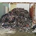
廢棄物清除

碳棒頭處裡

混合五金回收買賣

廢玻璃處理

馬達回收買賣
廢玻璃處理

廢棄物處裡

建築廢棄物處理

面板玻璃處理
上一頁下一頁
分享:


相片最新留言
參加的共同相簿集

相簿所有人物
相簿列表資訊
- 最新上傳:
- 2024/05/02
- 全站分類:
- 不設分類
- 本日人氣:
- 0
- 累積人氣:
- 285

常見的半導體材料有矽、鍺、砷化鎵等
/
晶片測試
晶片處理高度有序化的本質增加了對不同處理步驟之間度量方法的需求。晶片測試度量裝置被用於檢驗晶片仍然完好且沒有被前面的處理步驟損壞。如果If the number of dies—the 積體電路s that will eventually become chips—當一塊晶片測量失敗次數超過一個預先設定的閾值時,晶片將被廢棄而非繼續後續的處理製程。
/
晶片測試
晶片處理高度有序化的本質增加了對不同處理步驟之間度量方法的需求。晶片測試度量裝置被用於檢驗晶片仍然完好且沒有被前面的處理步驟損壞。如果If the number of dies—the 積體電路s that will eventually become chips—當一塊晶片測量失敗次數超過一個預先設定的閾值時,晶片將被廢棄而非繼續後續的處理製程。
/
步驟列表
晶片處理
濕洗
平版照相術
光刻Litho
離子移植IMP
蝕刻(干法蝕刻、濕法蝕刻、電漿蝕刻)
熱處理
快速熱退火Annel
熔爐退火
熱氧化
化學氣相沉積 (CVD)
物理氣相沉積 (PVD)
分子束磊晶 (MBE)
電化學沉積 (ECD),見電鍍
化學機械平坦化 (CMP)
IC Assembly and Testing 封裝測試
Wafer Testing 晶片測試
Visual Inspection外觀檢測
Wafer Probing電性測試
FrontEnd 封裝前段
Wafer BackGrinding 晶背研磨
Wafer Mount晶圓附膜
Wafer Sawing晶圓切割
Die attachment上片覆晶
Wire bonding焊線
BackEnd 封裝後段
Molding模壓
Post Mold Cure後固化
De-Junk 去節
Plating 電鍍
Marking 列印
Trimform 成形
Lead Scan 檢腳
Final Test 終測
Electrical Test電性測試
Visual Inspection光學測試
Baking 烘烤
/
有害材料標誌
許多有毒材料在製造過程中被使用。這些包括:
有毒元素摻雜物比如砷、硼、銻和磷
有毒化合物比如砷化三氫、磷化氫和矽烷
易反應液體、例如過氧化氫、發煙硝酸、硫酸以及氫氟酸
工人直接暴露在這些有毒物質下是致命的。通常IC製造業高度自動化能幫助降低暴露於這一類物品的風險。
/
Device yield
Device yield or die yield is the number of working chips or dies on a wafer, given in percentage since the number of chips on a wafer (Die per wafer, DPW) can vary depending on the chips' size and the wafer's diameter. Yield degradation is a reduction in yield, which historically was mainly caused by dust particles, however since the 1990s, yield degradation is mainly caused by process variation, the process itself and by the tools used in chip manufacturing, although dust still remains a problem in many older fabs. Dust particles have an increasing effect on yield as feature sizes are shrunk with newer processes. Automation and the use of mini environments inside of production equipment, FOUPs and SMIFs have enabled a reduction in defects caused by dust particles. Device yield must be kept high to reduce the selling price of the working chips since working chips have to pay for those chips that failed, and to reduce the cost of wafer processing. Yield can also be affected by the design and operation of the fab.
Tight control over contaminants and the production process are necessary to increase yield. Contaminants may be chemical contaminants or be dust particles. "Killer defects" are those caused by dust particles that cause complete failure of the device (such as a transistor). There are also harmless defects. A particle needs to be 1/5 the size of a feature to cause a killer defect. So if a feature is 100 nm across, a particle only needs to be 20 nm across to cause a killer defect. Electrostatic electricity can also affect yield adversely. Chemical contaminants or impurities include heavy metals such as Iron, Copper, Nickel, Zinc, Chromium, Gold, Mercury and Silver, alkali metals such as Sodium, Potassium and Lithium, and elements such as Aluminum, Magnesium, Calcium, Chlorine, Sulfur, Carbon, and Fluorine. It is important for those elements to not remain in contact with the silicon, as they could reduce yield. Chemical mixtures may be used to remove those elements from the silicon; different mixtures are effective against different elements.
Several models are used to estimate yield. Those are Murphy's model, Poisson's model, the binomial model, Moore's model and Seeds' model. There is no universal model; a model has to be chosen based on actual yield distribution (the location of defective chips) For example, Murphy's model assumes that yield loss occurs more at the edges of the wafer (non-working chips are concentrated on the edges of the wafer), Poisson's model assumes that defective dies are spread relatively evenly across the wafer, and Seeds's model assumes that defective dies are clustered together.[25]
Smaller dies cost less to produce (since more fit on a wafer, and wafers are processed and priced as a whole), and can help achieve higher yields since smaller dies have a lower chance of having a defect. However, smaller dies require smaller features to achieve the same functions of larger dies or surpass them, and smaller features require reduced process variation and increased purity (reduced contamination) to maintain high yields. Metrology tools are used to inspect the wafers during the production process and predict yield, so wafers predicted to have too many defects may be scrapped to save on processing costs.[26]